
 Product
 Brand
Brand Articles
 Tools
Tools
Selection and Optimization of Peripheral Components for DC-DC Boost Regulator
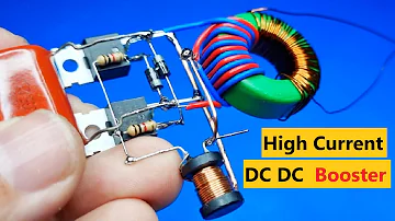
How To Make High Power DC DC Booster Circuit
RF transceivers, precision analog circuits, white LED backlight drivers, biasing avalanche photodiodes (APDs) circuits, and other operations that demand higher voltages are frequently found in battery-powered low-voltage applications such as portable and wearable electronics. This necessitates the employment of a DC-DC boost converter to up-convert to the appropriate voltage, allowing the device to function both efficiently and energy-efficiently.
Boost Regulator Features
Step-up DC-DC regulators transform low input voltages to high output voltages to fulfill some specific higher voltage requirements in low voltage applications. Inductors, power MOSFETs, rectifier diodes, control ICs, and input and output capacitors are all common circuit components.

Figure. 1 Basic Boost Regulator Configuration
A typical retrofit setup includes two MOSFETs. one of which substitutes the rectifier diode and switches on when the power switch is turned off. MOSFETs have a reduced voltage drop, which minimizes power dissipation while improving the regulator's efficiency.
Overtemperature, output short circuits, open load circumstances, and input overcurrent conditions are all protected by various regulators.
Peripheral component selection
The parasitic series resistance (ESR) of the inductor, the forward voltage drop of the Schottky diode, the on-resistance of the power tube, and the switch are the main sources of power loss in the DC-DC boost circuit. Of course, the chip's static power consumption would influence conversion efficiency under low load situations, thus the power tube's on-resistance must also be very low. Simultaneously, an appropriate driving circuit should be constructed inside the chip to ensure that the power tube's switching edge is very steep, reducing power consumption during switching.
The conversion efficiency will be affected by the choice of inductor and Schottky diode, and the output ripple will be affected by the choice of capacitor and inductance. High conversion efficiency, low ripple, and low noise can be achieved by using the right inductor, capacitor, and Schottky diode.
1. Inductor selection
The inductor is an important component of the boost converter because it stores energy during the on-time of the power switch and transfers it to the output during the off-time of the power switch via the output rectifier diode.
Designers must strike a compromise between inductor current ripple and efficiency. Lower inductance inductors have higher saturation current and lower series resistance for a given physical size, but lower inductance inductors have higher peak current, which results in lower energy efficiency, higher ripple, and higher noise.
The minimum inductance value Lmin, current ripple, and other factors influence the inductor's inductance value. Pay attention to the duty cycle (D) parameter when computing the specific inductance value; the specific size is D = (Vout-Vin)/Vout.
To begin, ensure that the minimum inductance value Lmin is met in order for the DC-DC boost to operate normally in continuous current mode.

Figure. 2
The actual value is greater because this formula is computed in the continuous current mode, ignoring additional conditions like as parasitic resistance and diode conduction voltage drop. If the inductance value is smaller than Lmin, the inductance may experience magnetic saturation, resulting in a significant reduction in the DC-DC circuit's efficiency, and even the steady voltage cannot be produced correctly
Second, in the continuous current mode, ignoring the parasitic parameters, investigate the current ripple problem across the inductor.

Figure. 3
When L is too tiny, the inductor's current ripple is too large, causing the chip's maximum current via the inductor, Schottky diode, and power tube to be too high. Because the power tube isn't perfect, when the current is exceptionally high, the power loss on the power tube increases, lowering the conversion efficiency of the overall DC-DC circuit.
Third, when efficiency is not taken into account, the load capacity of a tiny inductor is greater than that of a large inductor. The current ripple and maximum current value of the large inductance are tiny under the same load situation, therefore the high inductance can make the circuit start up at a lower input voltage (the above findings were determined under the same parasitic resistance conditions).
The operating frequency can be increased to lower the size of the external inductor. At a working frequency of 350KHz, for example, an inductance of more than 3.3uH is sufficient to ensure normal performance. However, if the output terminal needs to output a big current (for example, greater than 50mA), it is advised that a larger inductance be used to increase work efficiency.
In the case of a heavy load, the inductor's series resistance has a significant impact on conversion efficiency. The power loss in the inductor is roughly calculated as follows: Assuming that the inductor resistance is rL and the load resistance is Rload, the power loss in the inductor is roughly computed as follows:

Figure. 4
After careful research, a 27uH inductance of 0.5 is recommended. If you want to increase the efficiency of a large load, you should utilize an inductor with a higher inductance and a lower parasitic resistance.
2. Output capacitor selection
The output capacitor helps deliver a stable output voltage during load transients by reducing load ripple. When the ESR of the capacitor is taken into account, the ripple of the output voltage is:

Figure. 5
A somewhat large output capacitor value is necessary to lessen the output ripple. However, if the output capacitor is too large, the system's response time will be too slow, hence a 100uF capacitor is advised. Larger capacitors are necessary if less ripple is required.
The ripple induced by ESR becomes the most crucial element when the output is linked to a big load. Simultaneously, ESR will increase efficiency loss while decreasing conversion efficiency. As a result, low-ESR tantalum capacitors or numerous or X7R ceramic capacitors in parallel are preferred. Other capacitor types may have a greater ESR, which reduces converter efficiency.
3. Diode
The DC-DC efficiency is greatly influenced by the rectifier diode. Although regular diodes can make the DC-DC circuit work normally, the efficiency will be reduced by 5-10%. As a result, a diode with a low forward voltage and fast response time is preferred. 1N5817, 1N5819, 1N5821, 1N5822, and other turkey diodes
Specific parameters include the diode's average forward rated current being equal to or greater than the maximum output current, the repetitive peak forward rated current being equal to or greater than the peak inductor current, and the reverse breakdown voltage is greater than the internal power switch's rated voltage.
The MCP1665, for example, has a 36V internal switch that can deliver up to 1A. As a result, Microchip recommends utilizing the STMicroelectronics STPS2L40VU Schottky diode, which has a reverse breakdown voltage of 40V and a forward current of 2A.
4. Input capacitance
Even without the input filter capacitor, if the input power supply is stable, the DC-DC circuit can output current and voltage with low ripple and noise. When the power source is far away from the DC-DC circuit, however, it is advised that a filter capacitor of greater than 10uF be added to the DC-DC circuit's input end to reduce output noise.
DC-DC boost regulators have high-speed switching characteristics and are extremely sensitive to PCB layout: parasitic inductance and capacitance can result in high output ripple, poor output regulation, excessive electromagnetic interference (EMI), and even high voltage spikes, all of which can lead to failure. To decrease loop area, peripheral components should be close to the IC die, ground nodes should be close to the IC power ground pins, and power, signal, and thermal pads should all be connected at a single low-impedance ground point.
 UTMEL
UTMEL
We are the professional distributor of electronic components, providing a large variety of products to save you a lot of time, effort, and cost with our efficient self-customized service. careful order preparation fast delivery service
1. What is a DC/DC Boost Converter?
A DC-DC boost converter, also known as a boost converter or a DC boost chopper, is a DC-DC converter that boosts the voltage so that the output (load) voltage will be higher than the input (source) voltage.
2. What is the role of a DC/DC converter?
The DC/DC converter can perform high-frequency switching action through a controllable switch (MOSFET, etc.), and store the input electrical energy in the capacitor (inductance). When the switch is turned off, the electrical energy is released to the load to provide energy.
3. What is the difference between a DC-DC converter and a three-terminal regulator?
DC-DC converters are mostly used for high voltage or high power, and where the difference between the existing voltage and the conversion voltage is large, the three-terminal voltage regulator is mostly used for the required voltage and the existing voltage is not far from the difference, and low voltage, low voltage place of power.
 Discovering New and Advanced Methodology for Determining the Dynamic Characterization of Wide Bandgap DevicesSaumitra Jagdale15 March 20242594
For a long era, silicon has stood out as the primary material for fabricating electronic devices due to its affordability, moderate efficiency, and performance capabilities. Despite its widespread use, silicon faces several limitations that render it unsuitable for applications involving high power and elevated temperatures. As technological advancements continue and the industry demands enhanced efficiency from devices, these limitations become increasingly vivid. In the quest for electronic devices that are more potent, efficient, and compact, wide bandgap materials are emerging as a dominant player. Their superiority over silicon in crucial aspects such as efficiency, higher junction temperatures, power density, thinner drift regions, and faster switching speeds positions them as the preferred materials for the future of power electronics.
Read More A Comprehensive Guide to FPGA Development BoardsUTMEL11 September 202519083
This comprehensive guide will take you on a journey through the fascinating world of FPGA development boards. We’ll explore what they are, how they differ from microcontrollers, and most importantly, how to choose the perfect board for your needs. Whether you’re a seasoned engineer or a curious hobbyist, prepare to unlock new possibilities in hardware design and accelerate your projects. We’ll cover everything from budget-friendly options to specialized boards for image processing, delve into popular learning paths, and even provide insights into essential software like Vivado. By the end of this article, you’ll have a clear roadmap to navigate the FPGA landscape and make informed decisions for your next groundbreaking endeavor.
Read More 800G Optical Transceivers: The Guide for AI Data CentersUTMEL24 December 20258726
The complete guide to 800G Optical Transceiver standards (QSFP-DD vs. OSFP). Overcome supply shortages and scale your AI data center with Utmel Electronic.
Read More The 2026 Engineer’s Guide: Choosing the Right MCU for Your Next IoT & New Energy ProjectUTMEL30 April 2026594
A comprehensive comparison of 2026's leading MCUs from ST, NXP, and Microchip across power efficiency, processing performance, connectivity, and ecosystems to help engineers select the optimal chip for next-gen IoT and new energy projects.
Read More AI Server Components: Engineering Next-Gen Data Center Hardware for 100kW RacksUTMEL15 May 2026326
The transition from traditional enterprise IT to AI-driven workloads has rendered legacy data center hardware obsolete, forcing infrastructure planners to re-engineer server components for extreme thermal environments.
Read More
Subscribe to Utmel !
![TPD2S300YFFR]() TPD2S300YFFR
TPD2S300YFFRTexas Instruments
![ACPL-P340-000E]() ACPL-P340-000E
ACPL-P340-000EBroadcom Limited
![HCS360/SN]() HCS360/SN
HCS360/SNMicrochip Technology
![AD9972BBCZ]() AD9972BBCZ
AD9972BBCZAnalog Devices Inc.
![AD9970BCPZRL7]() AD9970BCPZRL7
AD9970BCPZRL7Analog Devices Inc.
![AT88SC25616C-PU]() AT88SC25616C-PU
AT88SC25616C-PUMicrochip Technology
![ACPL-336J-500E]() ACPL-336J-500E
ACPL-336J-500EBroadcom Limited
![ADUM3220WARZ]() ADUM3220WARZ
ADUM3220WARZAnalog Devices Inc.
![FM3164-G]() FM3164-G
FM3164-GCypress Semiconductor Corp
![HCS301-I/P]() HCS301-I/P
HCS301-I/PMicrochip Technology


